


Magasröptű gondolatoktól valamint "kékzoknit vettem fel ma reggel" jellegű posztoktól mentes jegyzettömb jellegű karakteres alapú tárhely szigorúan saját részre.
Notepad - Logoszféra fórum
üzenetek
hozzászólások
Windows 7 és SSD, két jó barát
"A korábbi ígéretekhez híven megérkezett az Intel notebook SSD-khez az új firmware, mely már lehetővé teszi a Windows 7 számára a meghajtó optimális kiaknázását. A hasonló előnyök elérése érdekében az Intel szoftveres támogatást ad a korábbi Windowsokhoz."
...és az optimális kiaknázás:
Intel pulls SSD Toolbox for killing drives under Windows 7
[ Szerkesztve ]
AMD ATI Chips Comparison Table (9200-tól)
nVidia Chips Comparison Table (GF4 MX 420-tól)
The Golden Era of 3D Acceleration - 1994 / 2003
Érdemes megnézni.
Úgy fest hogy egy kissé elsiették a publikálását. (NDA)
Ez megmaradt a Firefox-ban:
The C3 Revision
Just like its predecessor, the new Phenom II X4 965 BE runs at 3.4GHz, likewise, there are no changes in the cache architecture. Note, however, the new stepping (3) and the new revision code (RB-C3).
Idle State
Exactly like the older version, the new '965 BE C3" throttles back to a 4 x multiplier for an 800 MHz core clock if there is no load on the CPU.
North Bridge
At default setting, the NB is running at 2.0GHz.
Overclocking
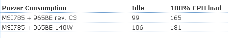
Whereas we had to resolve to somewhat arctic temperatures to squeeze 3.8GHz stable operation out of the previous revision, the C3 revision manages 4GHz at only a minor core voltage increase and air cooling at ambient room temperature.
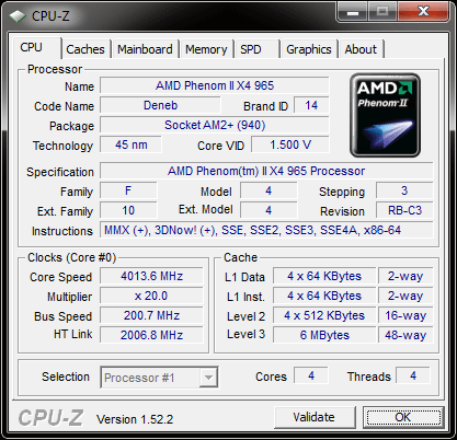
We were able to get into Win7 at 4.1 GHz but it would be exaggerating to claim stability at that speed. At 4.2 GHz, the CPU still reached the Windows7 desktop but crashed. Bear in mind that all of this was achieved using standard air cooling.
On the NB side of things, 3.0 GHz was also a breeze, and we achieved a score of 16783 in the multithreaded benchmark of Cinebench R10 (4.0GHz/3.0Ghz; 32 -bit binaries in Win7 64).
SATA 6G 6.0 Gb/s Performance Preview - Seagate XT drive tested
Remélem hogy idővel lesz belőle 1TB-os verzió is.
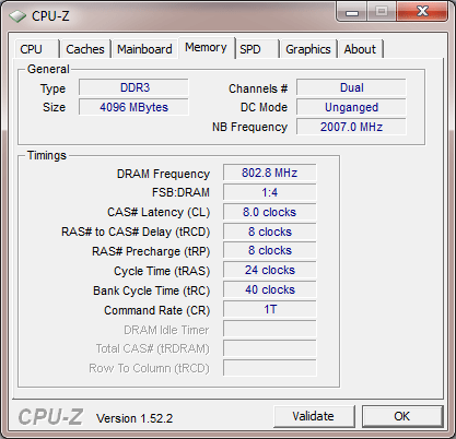
DDR
DDR400 CL3: 1000/200 = 5 -> 15,0 ns ciklusidő
DDR400 CL2,5: 1000/200 = 5 -> 12,5 ns ciklusidő
DDR400 CL2: 1000/200 = 5 -> 10,0 ns ciklusidő
DDR500 CL2,5: 1000/250 = 4 -> 10,0 ns ciklusidő
DDR500 CL2: 1000/250 = 4 -> 8,0 ns ciklusidő
DDR550 CL2: 1000/275 = 4 -> 7,272 ns ciklusidő
DDR600 CL2,5: 1000/300 = 3,33 -> 8,325 ns ciklusidő
DDR600 CL3: 1000/300 = 3,33 -> 9,99 ns ciklusidő
DDR2
DDR2-667 CL5: 1000/333 = 3 -> 15,0 ns ciklusidő
DDR2-667 CL4: 1000/333 = 3 -> 12,0 ns ciklusidő
DDR2-800 CL5: 1000/400 = 2,5 -> 12,5 ns ciklusidő
DDR2-800 CL4: 1000/400 = 2,5 -> 10,0 ns ciklusidő
DDR2-1066 CL5: 1000/533 = 1,87 -> 9,38 ns ciklusidő
DDR2-1066 CL4: 1000/533 = 1,87 -> 7,5 ns ciklusidő
DDR2-1200 CL5: 1000/600 = 1,66 -> 8,3 ns ciklusidő
DDR2-1200 CL4: 1000/600 = 1,66 -> 6,64 ns ciklusidő
DDR3
DDR3-1066 CL6: 1000/533 = 1,87 -> 11,22 ns ciklusidő
DDR3-1066 CL7: 1000/533 = 1,87 -> 13,1 ns ciklusidő
DDR3-1333 CL5: 1000/666 = 1,50 -> 7,5 ns ciklusidő
DDR3-1333 CL6: 1000/666 = 1,50 -> 9,0 ns ciklusidő
DDR3-1333 CL7: 1000/666 = 1,50 -> 10,5 ns ciklusidő
DDR3-1600 CL6: 1000/800 = 1,25 -> 7,5 ns ciklusidő
DDR3-1600 CL7: 1000/800 = 1,25 -> 8,75 ns ciklusidő
DDR3-1600 CL8: 1000/800 = 1,25 -> 10,0 ns ciklusidő
DDR3-1866 CL6: 1000/933 = 1,07 -> 6,42 ns ciklusidő
DDR3-1866 CL7: 1000/933 = 1,07 -> 7,49 ns ciklusidő
DDR3-1866 CL8: 1000/933 = 1,07 -> 8,56 ns ciklusidő
DDR3-2000 CL7: 1000/1000 = 1,00 -> 7,00 ns ciklusidő
DDR3-2000 CL8: 1000/1000 = 1,00 -> 8,00 ns ciklusidő
DDR3-2000 CL9: 1000/1000 = 1,00 -> 9,00 ns ciklusidő
DDR4
DDR4-2133 CL14: 1000/1066 = 0,94 -> 13,16 ns ciklusidő
DDR4-2133 CL15: 1000/1066 = 0,94 -> 14,10 ns ciklusidő
DDR4-2133 CL16: 1000/1066 = 0,94 -> 15,04 ns ciklusidő
DDR4-2400 CL15: 1000/1200 = 0,83 -> 12,45 ns ciklusidő
DDR4-2400 CL16: 1000/1200 = 0,83 -> 13,28 ns ciklusidő
DDR4-2400 CL17: 1000/1200 = 0,83 -> 14,11 ns ciklusidő
DDR4-2400 CL18: 1000/1200 = 0,83 -> 14,94 ns ciklusidő
DDR4-2666 CL17: 1000/1333 = 0,75 -> 12,75 ns ciklusidő
DDR4-2666 CL18: 1000/1333 = 0,75 -> 13,50 ns ciklusidő
DDR4-2666 CL19: 1000/1333 = 0,75 -> 14,25 ns ciklusidő
DDR4-2666 CL20: 1000/1333 = 0,75 -> 15,00 ns ciklusidő
DDR4-2933 CL19: 1000/1467 = 0,68 -> 12,92 ns ciklusidő
DDR4-2933 CL20: 1000/1467 = 0,68 -> 13,60 ns ciklusidő
DDR4-2933 CL21: 1000/1467 = 0,68 -> 14,28 ns ciklusidő
DDR4-2933 CL22: 1000/1467 = 0,68 -> 14,93 ns ciklusidő
DDR4-3200 CL20: 1000/1600 = 0,63 -> 12,60 ns ciklusidő
DDR4-3200 CL22: 1000/1600 = 0,63 -> 13,86 ns ciklusidő
DDR4-3200 CL24: 1000/1600 = 0,63 -> 15,12 ns ciklusidő
DDR4-3200 CL14: 1000/1600 = 0,63 -> 8,82 ns ciklusidő
DDR4-3200 CL15: 1000/1600 = 0,63 -> 9,45 ns ciklusidő
DDR4-3200 CL16: 1000/1600 = 0,63 -> 10,08 ns ciklusidő
DDR4-3733 CL16: 1000/1867 = 0,59 -> 8,57 ns ciklusidő
DDR4-3733 CL17: 1000/1867 = 0,59 -> 9,10 ns ciklusidő
DDR4-4000 CL15: 1000/2000 = 0,50 -> 7,50 ns ciklusidő
DDR4-4000 CL16: 1000/2000 = 0,50 -> 8,00 ns ciklusidő
DDR4-4000 CL17: 1000/2000 = 0,50 -> 8,50 ns ciklusidő
DDR4-4000 CL18: 1000/2000 = 0,50 -> 9,00 ns ciklusidő
DDR4-4133 CL16: 1000/2066 = 0,48 -> 7,74 ns ciklusidő
DDR4-4266 CL16: 1000/2133 = 0,47 -> 7,50 ns ciklusidő
[ Szerkesztve ]
VIA Introduces New VIA Nano 3000 Series Processors
"With a host of advanced features including 64-bit support, advanced CPU virtualization technology, SSE4 for enhanced multimedia processing, and the industry-leading encryption and security capabilities integrated in the VIA PadLock Security Engine, VIA Nano 3000 Series processors also provide a secure, high-performance solution for emerging cloud-based computing environments."
Az ION-nal majd egész jó kis kombó lehet.
[ Szerkesztve ]
John Fruehe - Director of Business Development for Server/Workstation AMD:
You are mistaken about TDP, because both companies deal with it differently.
Intel has 2 power levels: TDP and max power, (and now a third, "sustained power").
Take a look at the X5570 to see: [link]
Maximum power dissipation (W) 197.97; 155.56 (sustained)
Thermal Design Power (W) 95
So the way Intel always measured it in the past, Max power is the maximum power that a CPU can draw. Every transistor firing in a worst case scenario.
TDP is a de-rated value (used to be 80%, but it has been creeping down which is bad). Intel would take the maximum power, assume that the processor would throttle the clock down and then take that measurement (of a throttled processor) as the "TDP".
Since that time they have added a maximum sustained, maybe you can ask them what that means. I am assuming that max power is a spike power and that sustained is something that lasts more than a few milliseconds.
Regardless, the maximum power that the processor could conceivably draw is 197W.
Our TDP is equivalent to their max power, it is the maximum power the processor could draw, every transistor firing in a worst case scenario.
Our ACP is average CPU power. We run standard workloads, run them at 100% utilization and measure power.
Intel is not real open about max power. They used to post it online, but when they started getting pressure from AMD about those max power ratings, they stopped showing up online.
I'd love to have someone from Intel come here to debate this topic, because at this point, the specs (which they try to keep private) are not in their favor.
In designing a system to max power (which you have to do), we are not 42w disavantaged, we are actually 60w advantaged.
We do release max power. It is called TDP.
The reason the thermal design sheet lists TDP is because that is what you use to design systems. TDP is designed for system builders and OEMs. ACP is designed for customers in figuring out what they need for the data center.
ACP came into being a few years back because our TDP was 95W and it was rare that we ever had a part that even got above 50W. Customers were complaining that they were budgeting their racks for a certian amount of power, assuming 95W, and then ending up heavily under utilized. We were getting a lot of complaints from customers that we were too conservative and that this was leading to too much inefficiency in their data centers. I was on the receiving end of a lot of these conversations and they were not pleasant as data center floor space was the most expensive real estate in the building.
If you want a simple rule of thumb, use the following.
Most power a system can draw:
Intel = Max power
AMD = TDP
Typical power draw for standard applications:
Intel = TDP
AMD = ACP
If you are asking "why doesn't AMD just use TDP like the rest of the world" then you are on to something. We actually do. If you bother to go back to the wikipedia link above, you'll see TDP defined as:
"The thermal design power (TDP), sometimes called thermal design point, represents the maximum amount of power the cooling system in a computer is required to dissipate"
That sounds a lot like how AMD defines TDP, but that also sounds like how Intel defines max power. So, in reality, the "hoky" measurement is actually Intel's TDP because it does not represent what the rest of the industry means when they say TDP.
Cuomo Files Federal Antitrust Suit Against Intel
For example, Intel is accused of paying I.B.M. $130 million to hold back on selling a server based on A.M.D.’s Opteron chip, while also threatening to curtail joint projects if I.B.M. marketed A.M.D.’s products. “The question is, can we afford to accept the wrath of Intel?” an I.B.M. executive wrote in a 2005 e-mail message, according to Mr. Cuomo’s office.
A similar e-mail message from an unnamed Hewlett-Packard executive talks about Intel planning to “punish” the company for selling products based on A.M.D.’s chips.
AMD OverDrive™ Utility 3.1.0 (2009-9-20) Update list:
1. Added support for AMD Phenom II X4 965BE CPU
2. Added support for ATI DX11 “Evergreen” graphic cards
3. Added support for additional super IO chip: IT8712
4. Added support for AMD S1g4 and ASB2 socket type CPUs
5. Enhanced the fan speed control and hardware monitoring feature
6. Enhanced AMD Smart Profiles feature
7. Improved the CPU core multiplier settings method to change only the settings of the highest P-state
8. Enhanced the apply settings mechanism for memory timings by only applying the settings that were changed
9. Fixed a bug in AODDriver
10. Fixed the bug that GPU usage cannot be retrieved even with the latest graphic driver

Revision Guide for AMD Family 10h Processors 3.60
[ Szerkesztve ]
First DirectCompute Benchmark Released
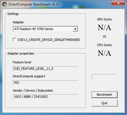
A forum member by the name of Pat has recently released a new benchmark tool for DirectCompute. This tool allows you to benchmark DirectX 11 latest general-purpose computing feature by calculating tons of FFT-like data and some memory transfers. DirectCompute is an application programming interface (API) that takes advantage of the massively parallel processing power of a modern graphics processing unit (GPU) to accelerate PC application performance. Be advised that DirectX 11 and the latest display drivers are required to run this benchmark.
Update: A new version (0.25) is now available.
Download this file in our downloads section.
Dirk Meyer, President and Chief Executive Officer
Nigel Dessau, Senior Vice President and Chief Marketing Officer
Emilio Ghilardi, Senior Vice President and Chief Sales Officer
Rick Bergman, Senior Vice President and General Manager, Products Group
Chekib Akrout, General Manager, Technology Group
Thomas Seifert, Senior Vice President and Chief Financial Officer
Highlights 
[ Módosította: Thrawn ]
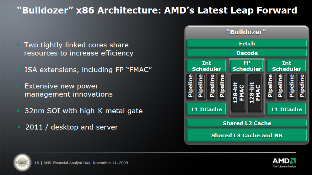
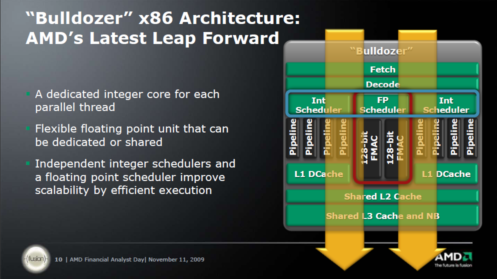
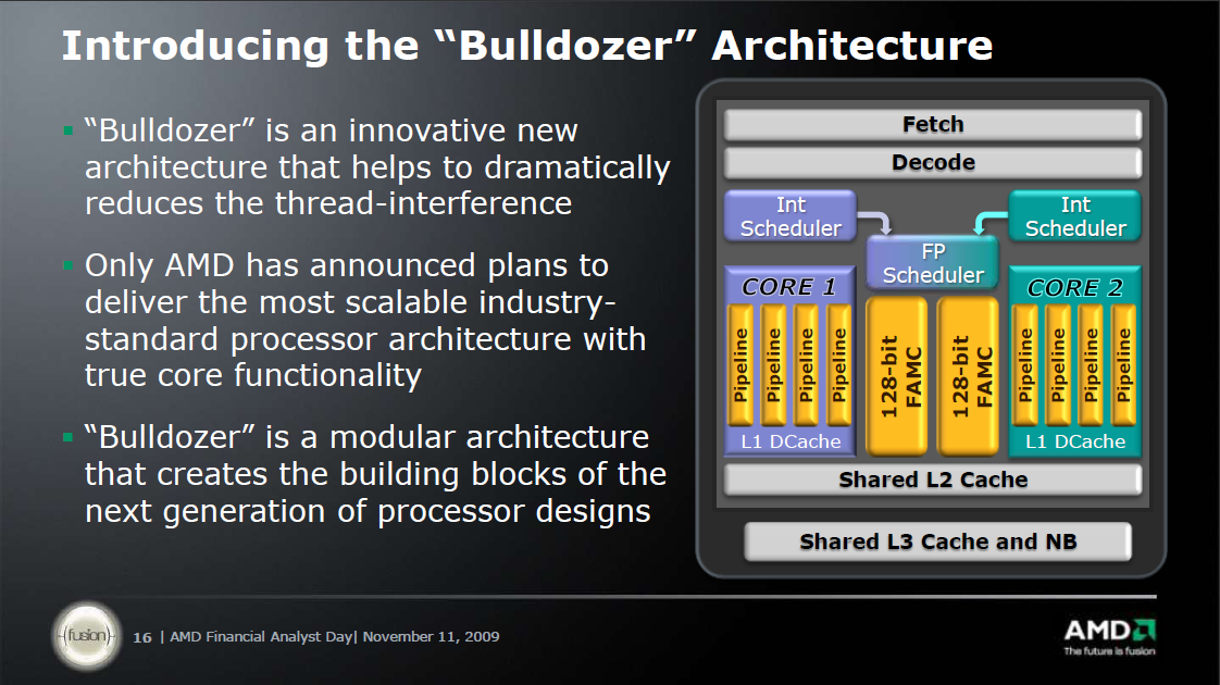
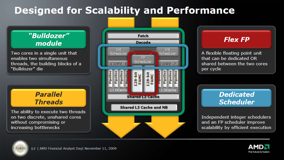
"Interesting to note are the "two tightly linked cores" sharing ressources. The shared FPU (which seems to be capable of 1x256 bit FMAC or 2x128 bit FMAC/FADD/FMUL in any combination per cycle) has been proposed many years ago by Fred Weber (AMD's CTO at that time). He already said, that two cores might share a FPU sitting between them. The whole thing is a CMT capable processor as speculated before. And if we look at core counts of Bulldozer based MPUs we should remember, that 2 such cores are accompanied by 1 FPU and an 8 core Zambezi actually contains 4 of these blocks shown on the Bulldozer slide.
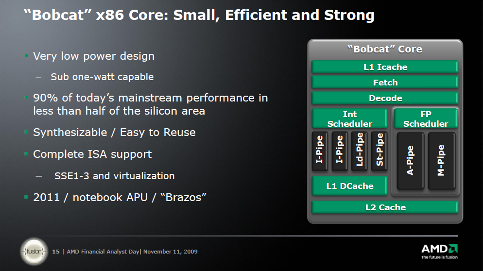
Further the 4 int pipelines per core/cluster aren't further detailed, while for Bobcat they are. In the latter case we see 2 ALU + 1 Store + 1 Load pipes. For BD I still think, that we'll see 2 ALU + 2 AGU (combined Load/Store) pipes. Those "multi mode" AGUs would simply fit better to achieve a higher bandwidth and be more flexible, because the FPU will also make use of these pipes. BTW compared to the combined 48B/cycle L1 bandwidth (could be used e.g. as 48B load bandwidth) of Sandy Bridge we might only see 32B/cycle L1 bandwidth per core but up to 64B/cycle combined L1 bandwidth per FPU (although shared by 2 threads). Finally, nobody knows clock speeds of these processors, so no real comparison is possible right now.
Today rumour site Fudzilla posted some rumoured details of BD, e.g. DDR3-1866 compatibility, 8 MB L3 (for 8 cores) and "APM Boost Technology". A german site even mentioned some mysterious patents pointing into the same direction... Well, given the time frame and filing dates I see both a chance for a simple core level overclocking like Intels Turbo Boost, because this is covered in AMD patents and a chance for a more complex power management on a core component level as described in my second last blog posting."
"Take the current decoders and add a fourth. This would work most of the time but would work better if you add another small buffer between the predecode and decode stages or if you increase the depth of the pick buffer. Then you continue with 4 pipelines to the reorder buffer and down to four dispatch and four ALU/AGU units. You can't break these apart without redesigning the front end decoder and the dispatch units.
The FMAC units are now twice as fast so you really don't need more than two per pair of cores. Besides you can't keep the same ratio while doubling the speed without busting your thermal limits. Even at that, the L1 Data bus is too small. So, you double the width of the L2 cache bus and get your SSE data directly from there. This leaves the existing L1 Data caches to service the Integer units. That increases the data bandwidth by 50%. The current limit is two 128 bit loads per core. If we allow the same for FP then we have six 128 bit loads per core pair. The current limit is two 64 bit saves per core. They could leave this unchanged on the integer side and beef up the FP unit to allow two 128 bit loads, one 128 bit load plus one 128 bit save, or two 128 bit saves. That would give the FP sufficient bandwidth. The front end doesn't really have to be changed since current FP instructions are already sent to another bus. It's a good question of whether each core gets one FMAC all to itself or whether they can intermingle. Either would be possible since threading the FP pipeline would only require extra tags to tell the two threads apart. Two threads would also break some dependencies and partially make up for the extra volume due to tighter pipeline packing and fewer stalls.
Presumably, widening the pipelines to four would give a good boost to Integer performance. I suppose 33% would be the max unless they beef up the decoders but 20% would be enough. I'm guessing they would also change the current behavior of the decoders which now tend to stall when when decoding complex instructions and would probably reduce the decode time on more of the Integer instructions.
The only reason for a complete redesign would be if the architecture extensions can't fit into the thermal limits."
"Each bulldozer module will have 2 integer cores and a shared FPU. When you consider that 80-90% of the work is integer, this is a great way to keep the performance up and reduce power consumption.
For those that said HT was such a great technology because for 5% more die space they get a 10-20% performance bump, the word from our engineers is that adding a second integer core to each bulldozer module is ~5% silicon but nets ~80% performance uplift over a single integer core.
I have been saying for a long time that the HT tradeoff was not worth it, this is why.
You'll see bulldozer-based products with generally the same power and thermals that you see on today's products, but with significantly more throughput."
John Fruehe
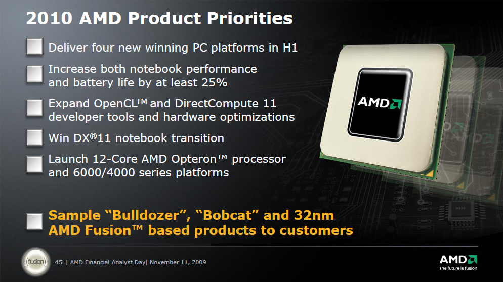
Journalist: Rick you mentioned that you will be sampling Bulldozer and Bobcat in 32nm, Fusion products in the first half of 2010. That would suggest that you either have taped out or is close to taping out all those products. Can you give us some sense off where you are in terms of the development on those cores?
Rick Bergman: We don't really give out inner milestones, but we, obviously you know how the semiconductor industry works. You know, June of 2010 is 7 months from now, it takes a few months to build these things so I don't think your comments are off-target at all we are, we're loading up the gun getting ready with our next wave of these fantastic products
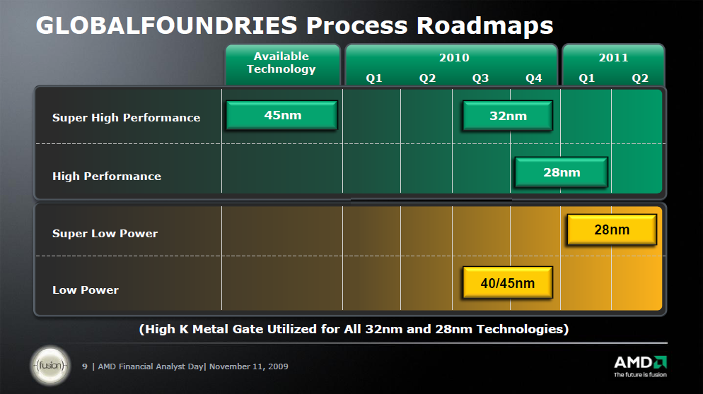
Journalist: You mentioned, I think the roadmap for Global Foundries showed that you had, that they were doing 32nm in the second half of 2010. So how do you actually get those built in the first half?
Dirk Meyer: That was a production question.
Emilio Ghiraldi: That's manufacturing ramp, which is consistent with the...
Journalist: So they are doing the tape-outs now?
Rick Bergman: Oh yeah, absolutely and we have running material, we have material
.
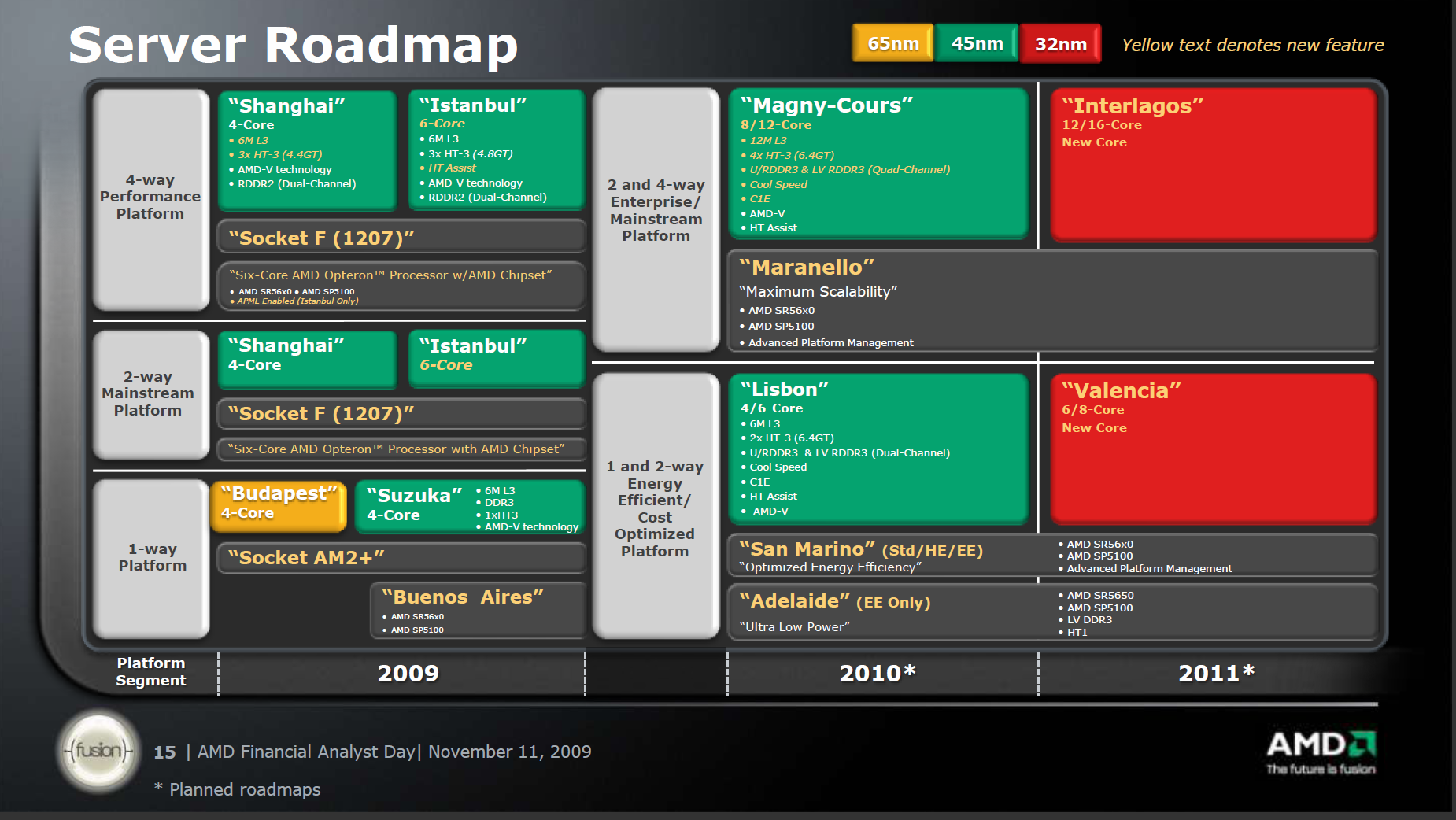
"C32 is a new socket but it is based on the physical 1207 mechanics. This means that all of the tooling and development costs for the socket have been amortized and it is at a low cost. And partners know how to deal with it because they have been laying out with 1207 for years.
We swapped some pin assignments so that we could support DDR-3 and higher capacities of memory, so current DDR-2 parts will not work in the new sockets. We added some keying on the socket to ensure that 1207 fits in 1207 and C32 fits in C32, no mixing. That reduces the test matrix for customers and prevents them from having to support DDR-3 on older parts."
John Fruehe
Summary:
- Intel has agreed to an important set of ground rules to a free and open market in the microprocessor industry
- New patent cross-license agreement that gives AMD broad rights and the freedom to operate a business utilizing multiple foundries
- GLOBALFOUNDRIES has agreed to terms that allow them the freedom to operate as an independent world-class leading-edge foundry company, going forward, without being a subsidiary of AMD.
- Intel has agreed to pay AMD $1.25 billion within 30 days of this agreement.
- AMD has agreed to drop all pending lawsuits against Intel as well as all regulatory complaints.
"Clarkdale" & "Arrandale" - Ahol a tákolás új értelmet nyer.
Két lapka egy nyákra ültetve akárcsak a Core 2 Quad esetében de itt ez utóbbitól eltérően a két lapka különböző csíkszélességgel készül. A CPU 32nm-en még a grafikus vezérlőt is tartalmazó lapka pedig még 45nm-en.
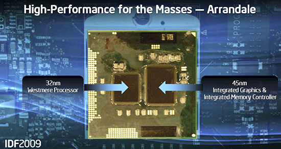
Ezzel még talán nem is lenne baj de bizonyos okból kifolyólag a memória vezérlő nem a CPU-ba került hanem maradt az IGP mellett. A CPU QPI-n keresztül csatlakozik az IGP + mem. vezérlő egységhez ami így ebben a formában meglehetősen hasonló a klasszikus FSB-s felépítéshez, csak az északi híd (jelen esetben az IGP + mem. vezérlő stb. kombó ami eléggé hajaz a G45-re) az alaplapról átköltözött a CPU nyákjára.
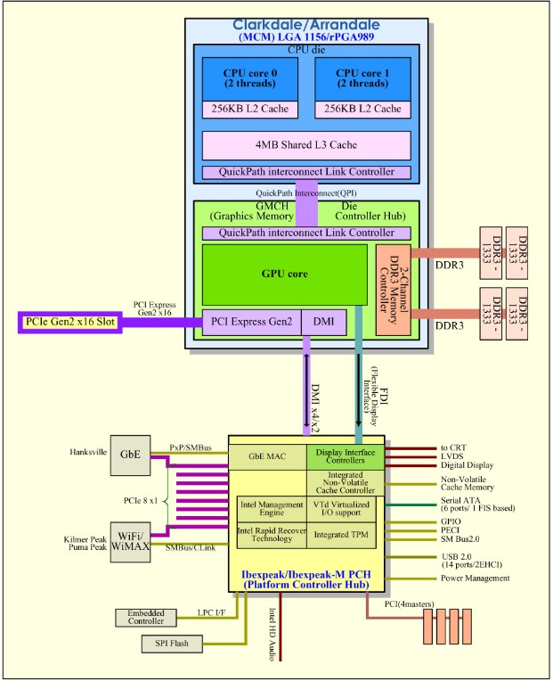
Tehát jelen esetben gyakorlatilag az FSB-t átkeresztelték QPI-re, csiszoltak egy kicsit a GMA 4500-on valamint egy nyákra rakták egy kiherélt/félbevágott és 32nm-en legyártott Bloomfield-vel így elkészült az új Clarkdale/Arrandale.
Értelemszerűen a 45nm-es rész még abban az esetben is üzemelni fog ha az IGP egyáltalán nem lesz kihasználva (pl.: P55-ös alaplapok), mivel azon kívül még ott van a memóriavezérlő is. Ezen felül a CPU-nak még át kell verekednie magát ezen a részen hogy eljusson a P55-ös PCH-hoz. A CPU-n kívül elhelyezkedő memória vezérlő pedig az FSB-s rendszerekhez hasonlóan nem lesz túl jó hatással a memória elérésre.
[ Szerkesztve ]
"A few points that I'd like to note down from Chuck Moore's presentation since they're not written onto the slides:
- Bulldozer will have improved single-thread performance than today's processors
- He seems to imply that at some point SIMD instructions may be offload to GPU, but it'll be the (post-2011) future era
- Larger cache, higher memory integration (stacked memory) are being considered for the future era
- Llano has CPU and GPU sharing the same memory controller(s)
- Llano will use currently existing (OpenCL & DirectCompute) programming model
- Llano will have the video processing & display subsystem and integrated PCIe bus
- Bobcat core(s) can be integrated with GPU and/or other peripheral functions in the computer
- Future generations of Bobcat will continue to have even lower power
- Each Bulldozer module is an optimized dual core
- Each Bulldozer "core" is capable of 2 loads/cycle; each is a 4-way out-of-order machine
- Bulldozer module is not bigger in area than Intel's hyperthreading design
- Bulldozer module can achieve ~80% speedup when running 2 threads (versus ~25% from hyperthreading)
- Multiple Bulldozer modules can share the L2 cache; and multiple of those (module? L2?) can share the L3 and NB
- Each INT scheduler can issue 4 inst./cycle; the FP scheduler can issue 4 inst./cycle
- "Over time" a Bulldozer "core" (INT only?) can be deployed in APU to work with GPGPU (for FP?)
Conclusion: Each Bulldozer core is 4-way INT and 2 to 4-way FP (depending on sharing), up from the 3-way each in K8/K10 today."
AMD shakes up x86 CPU world with two new designs
Interview with AMD's Fred Weber - The Future of AMD Microprocessors (March 31st, 2005)
How about a Hyper Threaded Athlon?
When Intel announced Hyper Threading, AMD wasn't (publicly) paying any attention at all to TLP as a means to increase overall performance. But now that AMD is much more interested and more public about their TLP direction, we wondered if there was any room for SMT a la Hyper Threading in future AMD processors, potentially working within multi-core designs.
Fred's response to this question was thankfully straightforward; he isn't a fan of Intel's Hyper Threading in the sense that the entire pipeline is shared between multiple threads. In Fred's words, "it's a misuse of resources." However, Weber did mention that there's interest in sharing parts of multiple cores, such as two cores sharing a FPU to improve efficiency and reduce design complexity. But things like sharing simple units just didn't make sense in Weber's world, and given the architecture with which he's working, we tend to agree.
[ Szerkesztve ]
